| CPC H01L 23/5386 (2013.01) [H01L 21/4853 (2013.01); H01L 23/481 (2013.01); H01L 24/16 (2013.01); H01L 24/48 (2013.01); H01L 25/16 (2013.01); H01L 23/5286 (2013.01); H01L 2224/16225 (2013.01); H01L 2224/48229 (2013.01); H01L 2924/16251 (2013.01)] | 20 Claims |
|
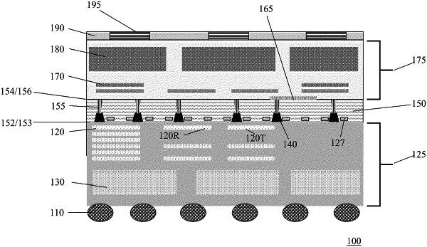
1. A semiconductor chip (chip) comprising:
one or more bottom external connections, one or more of the bottom external connections being a bottom external power connection and one or more of the bottom external connections being a bottom external ground connection;
a front side power network layer, the front side power network layer having one or more front side layers, one of the front side layers being a top front side, one or more of the front side layers having one or more front side power connections and one or more front side ground connections, one or more of the front side power connections electrically connected to one or more bottom external power connections and one or more of the front side ground connections connected to one or more of the bottom external ground connections;
at least one device layer, the device layer having a plurality of devices, one or more of the devices having one or more device power connections and one or more device ground connections, the device layer having a device layer front side and a device layer back grind side, the device layer front side being above and attached to the top front side layer, and one or more of the front side power connections electrically connected to one or more of the device power connections and one or more of the front side ground connections connected to one or more of the device ground connections;
a grind side power network layer, the grind side power network layer having one or more grind side layers, one of the grind side layers being a bottom grind side layer, the bottom grind side layer attached to and above the back grind side of the device layer, one or more of the grind side layers having one or more grind side power connections and one or more of the grind side layers having one or more grind side ground connections, one or more of the grind side power connections electrically connected to one or more of the device power connections and one or more of the grind side ground connections electrically connected to one or more of the device ground connections; and
one or more top external connections, one or more of the top external connections being a top external power connection and one or more of the top external connections being a top external ground connection, one or more of the top external power connections being connected to one or more of the grind side power connections and one or more of the top external ground connections being connected to one or more of the grind side ground connections,
wherein one or more first device power connections is connected to one of the bottom external power connections, one or more second device power connections is connected to one of the top external power connections, and one or more of the device around connections is connected to one of the bottom external ground connections and one of the top external ground connections.
|