| CPC H01L 23/528 (2013.01) [H01L 23/3192 (2013.01); H01L 23/522 (2013.01); H01L 27/0688 (2013.01); H10B 43/40 (2023.02); H01L 2924/0002 (2013.01); H10B 43/27 (2023.02)] | 20 Claims |
|
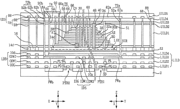
1. A semiconductor device, comprising:
a semiconductor substrate;
a first pattern on the semiconductor substrate;
a second pattern disposed at substantially the same level as the first pattern and spaced apart from the first pattern;
a peripheral circuit on the semiconductor substrate, at least a portion of the peripheral circuit being between the semiconductor substrate and the first pattern;
a dummy interconnection structure on the semiconductor substrate;
a stacked structure including cell gate conductive patterns on the first pattern, the cell gate conductive patterns being stacked while being spaced apart from each other in a vertical direction perpendicular to an upper surface of the first pattern;
a cell vertical structure disposed on the first pattern and passing through the cell gate conductive patterns, wherein at least one side of the stacked structure has a staircase shape; and
a dummy contact plug directly on and contacting the second pattern,
wherein a portion of the cell vertical structure directly contacts the first pattern,
wherein an upper end of the dummy contact plug is at a higher level than an uppermost cell gate conductive pattern among the cell gate conductive patterns,
wherein a lower end of the dummy contact plug is at a lower level than a lowermost cell gate conductive pattern among the cell gate conductive patterns,
wherein the dummy interconnection structure is electrically isolated,
wherein the dummy interconnection structure includes dummy patterns disposed at different levels from each other with respect to an upper surface of the semiconductor substrate,
wherein the dummy patterns include:
a first dummy pattern; and
a second dummy pattern disposed at a higher than the first dummy pattern,
wherein the peripheral circuit includes:
a first peripheral interconnection pattern disposed at substantially the same level as the first dummy pattern; and
a second peripheral interconnection pattern disposed at substantially the same level as the second dummy pattern.
|