| CPC H01L 23/49833 (2013.01) [H01L 23/3121 (2013.01); H01L 23/49811 (2013.01); H01L 23/49822 (2013.01)] | 13 Claims |
|
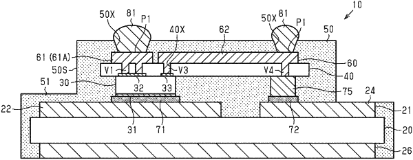
1. A semiconductor device, comprising:
a lower substrate;
a semiconductor element mounted on an upper surface of the lower substrate;
an upper substrate disposed on an upper surface of the semiconductor element;
an encapsulation resin disposed between the lower substrate and the upper substrate and encapsulating the semiconductor element;
a wiring layer disposed on an upper surface of the upper substrate; and
a covering resin formed from a material having a coefficient of thermal expansion similar to a coefficient of thermal expansion of the encapsulation resin,
wherein the covering resin is disposed on the upper surface of the upper substrate,
wherein the covering resin covers a side surface of the wiring layer and an upper surface of the wiring layer and includes an opening that partially exposes the upper surface of the wiring layer,
wherein the upper substrate includes a substrate body and an adhesive layer formed on a lower surface of the substrate body, and the upper surface of the semiconductor element is adhered to the substrate body by the adhesive layer, and
wherein the wiring layer has a thickness that is greater than that of the substrate body.
|