| CPC H01L 23/49822 (2013.01) [H03F 3/213 (2013.01); H05K 1/111 (2013.01); H05K 1/16 (2013.01); H05K 1/181 (2013.01); H05K 1/185 (2013.01); H05K 1/0231 (2013.01); H05K 1/0233 (2013.01)] | 28 Claims |
|
1. A substrate comprising:
an encapsulation layer;
a capacitor device located in the encapsulation layer, wherein the capacitor device comprises:
a capacitor substrate;
a first capacitor metal layer;
an insulator layer coupled to the first capacitor metal layer;
a second capacitor metal layer coupled to the insulator layer such that the insulator layer is located between the first capacitor metal layer and the second capacitor metal layer; and
at least one capacitor device dielectric layer;
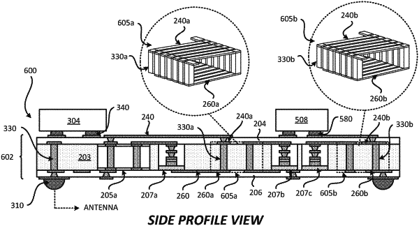
an inductor located in the encapsulation layer;
at least one first dielectric layer coupled to a first surface of the encapsulation layer; and
a plurality of first interconnects coupled to the first surface of the encapsulation layer,
wherein the plurality of first interconnects is located at least in the at least one first dielectric layer, and
wherein the plurality of first interconnects is coupled to the capacitor device and the inductor.
|