| CPC H01L 23/49816 (2013.01) [H01L 23/66 (2013.01); H05K 1/0228 (2013.01); H05K 3/3436 (2013.01); H01L 2223/6605 (2013.01); H05K 2201/09227 (2013.01); H05K 2201/10098 (2013.01); H05K 2201/10734 (2013.01)] | 30 Claims |
|
1. An apparatus, comprising:
a first semiconductor die stacked vertically relative to a layer of a printed circuit board (PCB), the first semiconductor die coupled to the PCB with a ball grid array (BGA);
a second semiconductor die stacked vertically relative to the layer of the PCB, the second semiconductor die coupled to the PCB with a BGA;
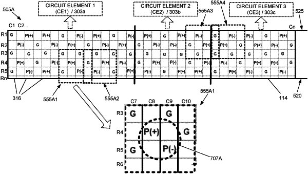
a pin map corresponding to each BGA and covering a surface area of the PCB, the pin map comprising a plurality of electrical designations for each pin in the pin map and a plurality of empty spaces within the pin map; each electrical designation of the plurality of electrical designations on the pin map comprising one of a positive polarity (P+), a negative polarity (P−), or an electrical ground (G);
each pin map including a first repeating pin polarity pattern; the first repeating pin polarity pattern comprising a lane unit tile, the lane unit tile having a central region defined by four pin map units, two of the four pin map units comprising two pins corresponding to a signal lane within the PCB.
|