| CPC H01L 23/49811 (2013.01) [H01L 21/4817 (2013.01); H01L 21/4853 (2013.01); H01L 23/552 (2013.01); H01L 23/66 (2013.01); H01L 24/48 (2013.01); H01Q 1/2283 (2013.01); H01L 2223/6677 (2013.01); H01L 2224/48227 (2013.01)] | 15 Claims |
|
1. A method, comprising:
mounting at least one electronic integrated circuit chip on a bearing surface of a support substrate;
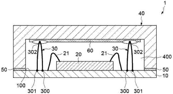
fixing first ends of a plurality of U-shaped metal wires onto the bearing surface at a side of said at least one electronic integrated circuit chip;
forming a metallic pattern at least on an internal wall of a non-conductive encapsulation cover;
locally forming a portion of solder on said metallic pattern;
mounting the non-conductive encapsulation cover on said bearing surface of the support substrate such that the internal wall is positioned opposite the bearing surface and second ends of the U-shaped metal wires are in contact with the locally formed portion of solder; and
after mounting, raising a temperature of said locally formed portion of solder so as to effectuate a soldering of said second ends of the U-shaped metal wires onto the metallic pattern.
|