| CPC H01L 23/367 (2013.01) [H01L 23/3736 (2013.01); H01L 24/06 (2013.01); H01L 24/09 (2013.01); H01L 24/17 (2013.01); H01L 2924/014 (2013.01); H01L 2924/0105 (2013.01); H01L 2924/01029 (2013.01); H01L 2924/01047 (2013.01); H01L 2924/01049 (2013.01); H01L 2924/01083 (2013.01); H01L 2924/15311 (2013.01)] | 15 Claims |
|
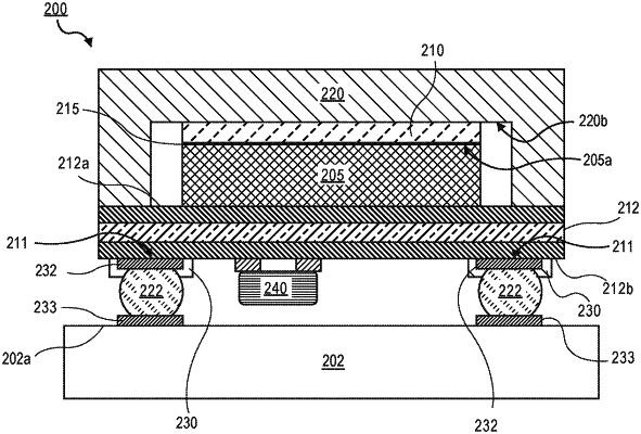
1. A semiconductor package, comprising:
a die on a top surface of a package substrate;
an integrated heat spreader (IHS) on the top surface of the package substrate, wherein the IHS has a bottom surface positioned above the die;
a solder thermal interface material (STIM) coupling a top surface of the die to the bottom surface of the IHS;
a low-temperature solder (LTS) paste comprising an alloy including tin (Sn) and bismuth (Bi), the LTS paste on a bottom surface of the package substrate, wherein the LTS paste has a weight percentage of the Bi that is greater than approximately 43%, and wherein the LTS paste has a melting point that is 10° C. to 15° C. less than a melting point of the STIM; and
a solder ball on the LTS paste on the bottom surface of the package substrate, wherein the solder ball is in direct physical contact with the LTS paste.
|