| CPC H01L 22/12 (2013.01) [G06T 7/13 (2017.01); G06T 7/136 (2017.01); H01L 24/75 (2013.01); H01L 24/81 (2013.01); H04N 5/33 (2013.01); G06T 2207/10048 (2013.01); G06T 2207/20164 (2013.01); G06T 2207/30148 (2013.01); H01L 2224/75263 (2013.01); H01L 2224/75901 (2013.01); H01L 2224/812 (2013.01); H01L 2224/81908 (2013.01)] | 25 Claims |
|
1. A method of making a semiconductor device, comprising:
providing a semiconductor die;
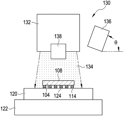
disposing a laser-assisted bonding (LAB) assembly including an infrared (IR) camera over the semiconductor die;
capturing an image of the semiconductor die using the IR camera;
performing image processing on the image to identify corners of the semiconductor die; and
identifying regions of interest (ROI) in the image relative to the corners of the semiconductor die.
|