| CPC H01L 21/823462 (2013.01) [H01L 21/02271 (2013.01); H01L 21/31111 (2013.01); H01L 21/31116 (2013.01); H01L 21/32135 (2013.01); H01L 21/823425 (2013.01); H01L 21/823437 (2013.01); H01L 27/088 (2013.01); H01L 29/1095 (2013.01); H01L 29/42368 (2013.01); H01L 29/66681 (2013.01); H01L 29/7816 (2013.01)] | 8 Claims |
|
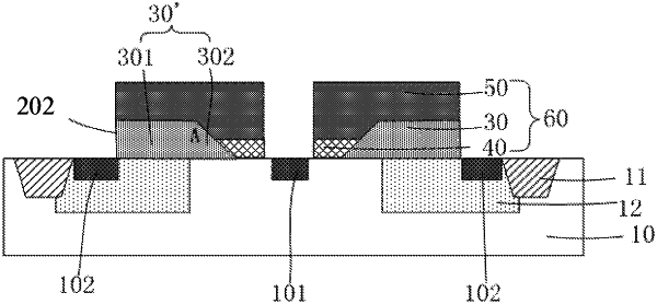
1. A semiconductor device, comprising:
a substrate;
a gate structure, located over the substrate, the gate structure including a first gate oxide layer, a second gate oxide layer, and a silicon layer, wherein:
the first gate oxide layer is over the substrate, and the first gate oxide layer has a sloped sidewall on one side and a vertical sidewall on another side, the first gate oxide layer including silicon oxide, and the sloped sidewall of the first gate oxide layer being covered by a by-product produced by an anisotropic dry etching using an etching gas with high fluorocarbon ratio;
the second gate oxide layer is over the substrate and on the sloped sidewall of the first gate oxide layer, and a thickness of the second gate oxide layer is less than a thickness of the first gate oxide layer, the second gate oxide layer including silicon oxide; and
the silicon layer is formed over the first gate oxide layer and the second gate oxide layer.
|