| CPC H01L 21/8222 (2013.01) [H01L 21/26513 (2013.01); H01L 27/0664 (2013.01); H01L 29/0649 (2013.01); H01L 29/66174 (2013.01); H01L 29/66242 (2013.01); H01L 29/7371 (2013.01); H01L 29/93 (2013.01)] | 18 Claims |
|
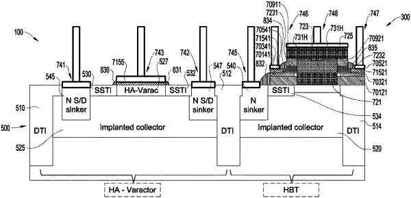
1. An integrated circuit, comprising:
a substrate;
a first collector region in said substrate doped with a first conductivity type;
a second collector region in said substrate also doped with the first conductivity type;
wherein the first collector region is isolated from the second collector region by a deep trench isolation in the substrate;
wherein a portion of the first collector region at an upper surface of the substrate is delimited by a shallow trench isolation;
a doped region with the first conductivity type in said portion of the first collector region;
an intrinsic collector epitaxy region with the first conductivity type over the second collector region;
an intrinsic base epitaxy region with a second conductivity type over the intrinsic collector epitaxy region;
an emitter region with the first conductivity type over the intrinsic base epitaxy region;
an extrinsic base region with the second conductivity type in contact with and laterally extending from the intrinsic base region;
an epitaxy layer with the second conductivity type that includes a first layer portion on said doped region and a second layer portion in contact with the extrinsic base region;
a doped layer with the second conductivity type over the substrate and laterally isolated from the intrinsic collector epitaxy region, and wherein said second layer portion is in contact with the doped layer;
wherein said doped region and first layer portion form a hyperabrupt PN junction for a variable capacitance diode; and
wherein said intrinsic collector epitaxy region, intrinsic base epitaxy region and emitter region form a bipolar transistor.
|