| CPC H01L 21/76897 (2013.01) [H01L 21/76805 (2013.01); H01L 21/76808 (2013.01); H01L 21/76877 (2013.01); H01L 2221/1026 (2013.01); H10B 43/35 (2023.02)] | 24 Claims |

|
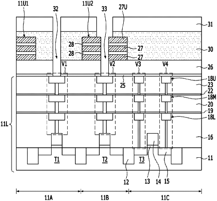
1. A method for fabricating a vertical memory device, the method comprising:
forming an alternating stack structure on a lower structure, wherein the alternating stack structure comprises first and second material layers alternately stacked with one another;
forming first and second alternating stack patterns by etching the alternating stack structure, wherein the first and second alternating stack patterns are isolated from each other by an isolation portion;
forming a through-hole penetrating through the second alternating stack pattern;
forming a first gap-fill layer, wherein the first gap-fill layer fills the isolation portion;
forming a second gap-fill layer, wherein the second gap-fill layer fills the through-hole;
forming a mask layer over the first and second alternating stack patterns and over the first and second gap-fill layers, wherein the mask layer comprises a hole type opening overlapping the first gap-fill layer and a self-aligned opening overlapping the filled through-hole and overlapping a portion of an uppermost material layer of the first and second material layers adjacent to the filled through-hole;
forming a first contact hole through the first gap-fill layer by performing a single etch using the mask layer as an etch barrier to remove, through the hole type opening, a portion of the first gap-fill layer; and
forming a second contact hole through the second alternating stack pattern by performing the single etch using both the mask layer and the portion of the uppermost material layer as etch barriers to remove, through the self-aligned opening, the second gap-fill layer filling the through-hole.
|