| CPC H01L 21/764 (2013.01) [H01L 21/76831 (2013.01); H01L 29/1037 (2013.01); H10B 43/27 (2023.02)] | 16 Claims |
|
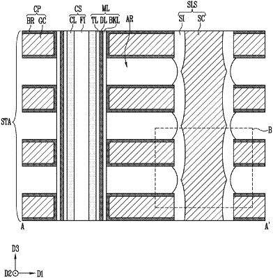
1. A semiconductor device comprising:
a stack structure including conductive patterns spaced apart from each other;
a channel structure penetrating the stack structure;
a slit insulating layer penetrating the stack structure in a first direction; and
a source contact in contact with the slit insulating layer,
wherein air gaps are defined between the conductive patterns,
wherein the slit insulating layer includes a first interposition part covering a sidewall of one of the conductive patterns and a second interposition part covering one of the air gaps from the side,
wherein a smallest width of the second interposition part in a second direction perpendicular to the first direction is smaller than a smallest width of the first interposition part in the second direction,
wherein the source contact includes a first contact part covering the first interposition part of the slit insulating layer and a second contact part covering the second interposition part of the slit insulating layer, and
wherein an interface between the first contact part of the source contact and the first interposition part of the slit insulating layer is convex towards the first contact part of the source contact.
|