| CPC H01L 21/76224 (2013.01) [H01L 21/7624 (2013.01); H01L 21/76227 (2013.01); H01L 21/76229 (2013.01); H01L 21/76232 (2013.01); H01L 21/76264 (2013.01); H01L 21/76283 (2013.01); H01L 27/1233 (2013.01); H01L 29/0653 (2013.01); H01L 29/786 (2013.01); H01L 29/78696 (2013.01)] | 20 Claims |
|
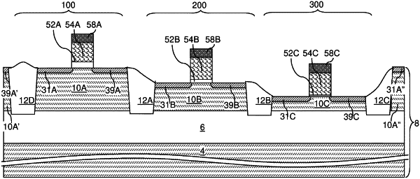
1. A method of forming a semiconductor structure, comprising:
providing a substrate including a top semiconductor layer that includes a first region, a second region, and a third region;
forming at least one first diffusion barrier layer that covers a first region of the top semiconductor layer and does not cover the second region and the third region of the top semiconductor layer;
thinning the second region and the third region of the top semiconductor layer without thinning the first region of the top semiconductor layer;
forming a second diffusion barrier layer that covers the first region and the second region of the top semiconductor layer and does not cover the third region of the top semiconductor layer;
additionally thinning the third region of the top semiconductor layer while a combination of the at least one first diffusion barrier layer and the second diffusion barrier layer masks the first region and the second region of the top semiconductor layer;
forming shallow trenches through the top semiconductor layer after said additional thinning of the third region of the top semiconductor layer;
forming a shallow trench isolation structure by filling the shallow trenches with a dielectric fill material and recessing portions of the dielectric fill material; and
forming semiconductor devices on discrete semiconductor portions in the first region and in the second region.
|