| CPC H01L 21/31116 (2013.01) [H01L 21/0212 (2013.01); H01L 21/0228 (2013.01); H01L 21/31144 (2013.01)] | 13 Claims |
|
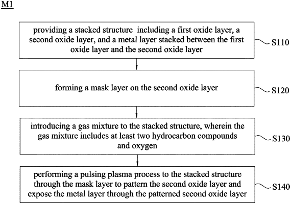
1. A method of manufacturing a semiconductor, comprising:
providing a stacked structure comprising a first oxide layer, a second oxide layer, and a metal layer stacked between the first oxide layer and the second oxide layer;
forming a mask layer on the second oxide layer;
introducing a gas mixture to the stacked structure, wherein the gas mixture comprises at least two hydrocarbon compounds and oxygen; and
performing a pulsing plasma process to the stacked structure through the mask layer to pattern the second oxide layer and expose the metal layer through the patterned second oxide layer,
wherein the forming the mask layer comprises:
forming a first covering layer on the second oxide layer; and
patterning the first covering layer to expose at least one portion of a surface of the second oxide layer, wherein the first covering layer comprises zirconium oxide or hafnium oxide.
|