| CPC H01L 21/0254 (2013.01) [H01L 21/0262 (2013.01); H01L 21/02381 (2013.01); H01L 21/02447 (2013.01); H01L 21/02458 (2013.01); H01L 29/04 (2013.01); H01L 29/2003 (2013.01); H01L 33/007 (2013.01); H01L 33/32 (2013.01)] | 9 Claims |
|
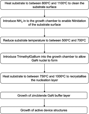
1. A method of manufacturing a semiconductor structure comprising a substantially (001) oriented zincblende structure group III-N layer, the method including the steps:
providing a silicon substrate;
providing a 3C—SiC layer on the silicon substrate;
subjecting the 3C—SiC layer to a nitridation step at a temperature T1 in the range 800-1100° C.;
growing a zincblende structure group III-N nucleation layer at a temperature T2 in the range 550-650° C. with a growth rate in the range 0.1-1 nm/s to a thickness in the range 10-100 nm;
carrying out a nucleation layer recrystallization step at a temperature T3 in the range 850-920° C.; and
depositing and growing the zincblende structure group III-N layer by MOVPE at temperature T3 in the range 850-920° C., to a thickness of at least 0.3 μm, wherein the group III-nitride layer is a In·sub·xAl·sub·yGa·sub·1-x-yN based layer, where 0≤x≤1, 0≤y≤1.
|