| CPC H01L 21/02274 (2013.01) [H01J 37/32146 (2013.01); H01L 21/0228 (2013.01); H01L 21/308 (2013.01); H01L 21/3065 (2013.01); H01L 21/67069 (2013.01); H01L 22/26 (2013.01)] | 13 Claims |
|
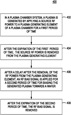
1. A method in a plasma chamber system for processing a wafer, comprising:
generating a plasma by applying RF source power to a plasma generating element of the plasma chamber for a first period of time of a pulse period of the RF source power;
after an expiration of the first period of time, removing the RF source power from the plasma generating element;
providing a delay after the removal of the RF source power and before an application of an RF bias signal;
controlling a length of the delay between the removal of the RF source power and the application of an RF bias signal to control a neutral density to ion density ratio for the plasma for determining a desired etch rate, etch depth, or etch selectivity for features on a surface of the wafer;
after the delay is controlled, applying an RF bias signal to bias the generated plasma towards the wafer for a second period of time during the pulse period of the RF source power; and
after an expiration of the second period of time, removing the RF bias signal before a next pulse period of the RF source power.
|