| CPC H01L 33/507 (2013.01) [H01L 25/167 (2013.01); H01L 33/502 (2013.01); H01L 2933/0041 (2013.01)] | 20 Claims |
|
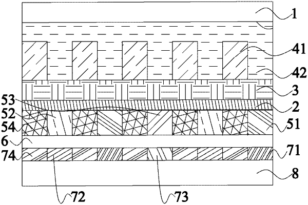
1. A display panel, comprising:
a first substrate;
a second substrate disposed opposite to the first substrate;
a driving circuit disposed opposite to the first substrate and adjacent to a side of the second substrate; and
a color resist layer disposed opposite to the driving circuit and adjacent to a side of the first substrate;
wherein the color resist layer comprises colorized color resist layers and a colorized quantum dot layer, the driving circuit is a bottom-emission type light-emitting-diode (LED) driving circuit, and quantum dots or scattering particles are disposed in the colorized quantum dot layer.
|