| CPC H01G 4/30 (2013.01) [H01G 2/02 (2013.01); H01G 4/008 (2013.01); H01G 4/012 (2013.01); H01G 4/1218 (2013.01); H01G 4/224 (2013.01); H01G 4/232 (2013.01); H01G 4/2325 (2013.01)] | 14 Claims |
|
1. A multilayer electronic component comprising:
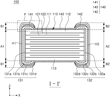
a body including dielectric layers, and first and second internal electrodes alternately stacked with respective dielectric layers interposed therebetween, the body having first and second surfaces opposing each other in a stacking direction, third and fourth surfaces connected to the first and second surfaces and opposing each other, and fifth and sixth surfaces connected to the first to fourth surfaces and opposing each other;
a first external electrode including a first electrode layer connected to the first internal electrode, a first conductive resin layer disposed on the first electrode layer, and a first plating layer disposed on the first conductive resin layer, and each having a first connection portion disposed on the third surface of the body and a first band portion extending from the first connection portion to a portion of each of the first, second, fifth, and sixth surfaces;
a second external electrode including a second electrode layer connected to the second internal electrode, a second conductive resin layer disposed on the second electrode layer, and a second plating layer disposed on the second conductive resin layer, and each having a second connection portion disposed on the fourth surface of the body and a second band portion extending from the second connection portion to a portion of each of the first, second, fifth, and sixth surfaces; and
a silicon (Si) organic compound layer having a body cover portion disposed on a region of external surfaces of the body between the first and second conductive resin layers, a first extending portion disposed to extend from the body cover portion to a region between the first band portion of the first conductive resin layer and the first band portion of the first plating layer, and a second extending portion disposed to extend from the body cover portion to a region between the second band portion of the second conductive resin layer and the second band portion of the second plating layer,
wherein the first and second conductive resin layers include a conductive metal and a base resin,
wherein at least one of the first or second extending portions has an opening through which the first plating layer contacts the first conductive resin layer or the second plating layer contacts the second conductive resin layer, respectively, and
wherein at least one of the first or second extending portions covers an end of a corresponding one of the first or second conductive resin layers.
|