| CPC H01G 4/2325 (2013.01) [H01G 4/008 (2013.01); H01G 4/012 (2013.01); H01G 4/248 (2013.01); H01G 4/30 (2013.01); H01G 4/1227 (2013.01)] | 14 Claims |
|
1. A multi-layered ceramic electronic component comprising:
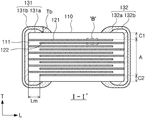
a ceramic body including a plurality of dielectric layers, and a plurality of internal electrodes opposing each other with the dielectric layers interposed therebetween, and including first and second surfaces opposing each other in a first direction corresponding to a stacking direction of the internal electrodes, third and fourth surfaces connected to the first and second surfaces and opposing each other in a second direction, and fifth and sixth surfaces connected to the first to fourth surfaces and opposing each other in a third direction; and
external electrodes disposed on the third and fourth surfaces on an exterior of the ceramic body and electrically connected to the internal electrodes,
wherein the ceramic body includes an active portion including the plurality of internal electrodes opposing each other with the dielectric layers interposed therebetween, to form capacitance, and cover portions formed above and below the active portion and free of the internal electrodes,
each external electrode includes an electrode layer disposed on the third and fourth surfaces to be electrically connected to at least some of the internal electrodes, and a conductive resin layer arranged on the electrode layer, the conductive resin layer extending to the first surface and the second surface of the ceramic body,
a ratio of a thickness (Tb) of the conductive resin layer extending to the first surface and the second surface of the ceramic body to a length (Lm) of a length direction margin portion of the ceramic body satisfies 2 to 29%,
a thickness (td) of the dielectric layers and a thickness (te) of the internal electrodes satisfy the relationship td>2×te, and
the thickness (Tb) of the conductive resin layer extending to the first surface and the second surface of the ceramic body is a maximum thickness among thicknesses of the conductive resin layer measured orthogonally to the first surface.
|