| CPC G11C 16/3431 (2013.01) [G11C 11/5628 (2013.01); G11C 11/5635 (2013.01); G11C 16/0416 (2013.01); G11C 16/0466 (2013.01); G11C 16/0483 (2013.01); G11C 16/0491 (2013.01); G11C 16/10 (2013.01); G11C 16/26 (2013.01); G11C 16/28 (2013.01); G11C 16/3427 (2013.01); H01L 27/0688 (2013.01); H01L 29/40117 (2019.08); H01L 29/66833 (2013.01); H01L 29/7926 (2013.01); H05K 999/99 (2013.01); H10B 43/27 (2023.02); H10B 43/40 (2023.02); H10B 43/10 (2023.02)] | 32 Claims |
|
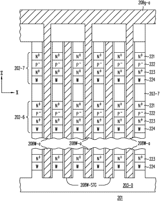
1. A memory structure, comprising:
a semiconductor substrate having a substantially planar surface and having circuitry formed therein and thereon;
an insulating layer over the semiconductor substrate;
a first stack of active strips and a second stack of active strips formed over the insulating layer and directly above the circuitry of the semiconductor substrate, wherein:
(i) each stack of active strips comprises two or more active strips provided one on top of another and electrically isolated from each other, the active strips (a) being substantially aligned lengthwise with each other along a first direction substantially parallel to the planar surface, and each comprising a semiconductor layer provided between a first conductive layer and a second conductive layer; and
(ii) the first stack and the second stack being separated from each other a predetermined distance along a second direction transverse to the first direction and parallel to the planar surface;
a data storage material provided on sidewalls of the first and second stacks;
a plurality of local conductors each extending lengthwise along a third direction that is substantially perpendicular to the planar surface, each local conductor being separated from one or both of the first and the second stacks by the data storage material; and
first global conductive wiring having conductors each running along the second direction for connecting the local conductors to the circuitry;
wherein each active strip further comprises a pre-charge transistor that is formed out of the semiconductor layer, the first and the second conductive layers of the active strip and a designated one of the local conductors that is adjacent to the active strip.
|