| CPC G11C 16/26 (2013.01) [G11C 11/5628 (2013.01); G11C 16/0483 (2013.01); G11C 16/08 (2013.01); G11C 16/10 (2013.01); G11C 16/14 (2013.01); G11C 16/349 (2013.01); G11C 16/3427 (2013.01)] | 20 Claims |
|
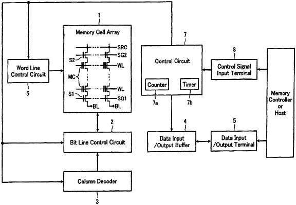
1. A method of performing a reading operation in a nonvolatile semiconductor memory device, the nonvolatile semiconductor memory device including a memory cell array which comprises: a memory string having a plurality of memory cells connected in series therein, each of the memory cells being configured programmable to plural written states from an erased state, the plural written states including a first state assigned to a lowest threshold voltage distribution among the plural written states; a first select transistor connected to one end of the memory string; a second select transistor connected to the other end of the memory string; a bit line connected to the memory string via the first select transistor; a source line connected to the memory string via the second select transistor; and a word line connected to a control gate electrode of each of the memory cells, the method of performing a reading operation being configured to apply a reading voltage to the control gate electrode of a selected memory cell in the memory string to determine whether the selected memory cell is conductive or not, and thereby execute data reading of the selected memory cell,
the method of performing a reading operation comprising:
performing a first reading operation including applying a source of the selected memory cell with a first voltage while applying the control gate electrode of the selected memory cell with the reading voltage and thereby determining whether a threshold voltage of the selected memory cell is in a range within the lowest threshold voltage distribution among the plural written states and over the lowest threshold voltage distribution; and
performing a second reading operation including applying the source of the selected memory cell with a second voltage with a positive value higher than a value of the first voltage while applying the control gate electrode of the selected memory cell with the reading voltage having a voltage value same as that of the reading voltage in the first reading operation and thereby determining whether the threshold voltage of the selected memory cell is in the range within the lowest threshold voltage distribution among the plural written states and over the lowest threshold voltage distribution.
|