| CPC G11C 16/10 (2013.01) [G06F 3/0625 (2013.01); G06F 3/0638 (2013.01); G06F 3/0679 (2013.01); G11C 16/26 (2013.01); G11C 11/56 (2013.01); G11C 16/0483 (2013.01)] | 20 Claims |
|
1. A method comprising:
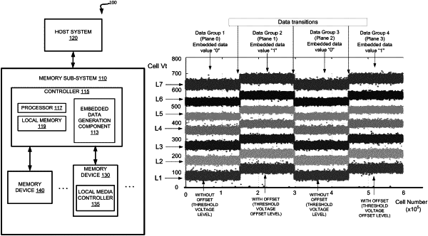
determining a target bit error rate corresponding to a point of a first programming voltage distribution level corresponding to memory cells of a memory sub-system and a second programming voltage distribution level corresponding to the memory cells of the memory sub-system;
selecting an offset voltage level corresponding to the point at the target bit error rate;
programming a first portion of a first group of the memory cells in the first programming voltage distribution level at a threshold voltage level to set a first embedded data value; and
programming a second portion of a second group of the memory cells in the second programming voltage distribution level at the threshold voltage level offset by the offset voltage level to set a second embedded data value.
|