| CPC G11C 16/08 (2013.01) [G11C 11/5628 (2013.01); G11C 11/5671 (2013.01); G11C 16/0483 (2013.01); G11C 16/10 (2013.01); G11C 16/16 (2013.01); G11C 16/24 (2013.01); G11C 16/26 (2013.01); G11C 16/3459 (2013.01); H01L 24/08 (2013.01); H01L 24/80 (2013.01); H01L 25/0657 (2013.01); H01L 25/18 (2013.01); H01L 25/50 (2013.01); H10B 41/10 (2023.02); H10B 41/27 (2023.02); H10B 41/35 (2023.02); H10B 41/41 (2023.02); H10B 43/10 (2023.02); H10B 43/27 (2023.02); H10B 43/35 (2023.02); H10B 43/40 (2023.02); H01L 2224/08145 (2013.01); H01L 2224/08146 (2013.01); H01L 2224/80895 (2013.01); H01L 2224/80896 (2013.01); H01L 2225/0651 (2013.01); H01L 2225/06506 (2013.01); H01L 2225/06517 (2013.01); H01L 2225/06524 (2013.01); H01L 2225/06541 (2013.01); H01L 2225/06562 (2013.01); H01L 2924/1431 (2013.01); H01L 2924/1438 (2013.01); H01L 2924/1443 (2013.01); H01L 2924/14511 (2013.01)] | 20 Claims |
|
1. A non-volatile storage apparatus, comprising:
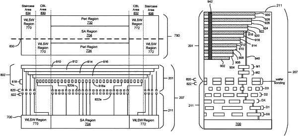
a three dimensional non-volatile memory structure that includes word lines connected to non-volatile memory cells;
one or more control circuits below the three dimensional non-volatile memory structure and configured to control the three dimensional non-volatile memory structure, the one or more control circuits include word line switch transistors, the one or more control circuits further include word line hook up signal lines connecting the word line switch transistors to word lines and pass through signal lines that provide electrical connections between components of the one or more control circuits, regions of the one or more control circuits are divided into a first set of regions and a second set of regions;
a first set of one or more metal line layers above the one or more circuits and below the three dimensional non-volatile memory structure; and
a second set of one or more metal line layers above the one or more circuits and below the three dimensional non-volatile memory structure, the first set of regions include word line hook up signal lines in the first set of one or more metal line layers and pass through signal lines in the second set of one or more metal line layers, the word line hook up signal lines are not included in the second set of one or more metal line layers in the first set of regions, the second set of regions include word line hook up signal lines in the first set of one or more metal line layers and in the second set of one or more metal line layers, the second set of regions further include pass through signal lines in the second set of one or more metal line layers.
|