| CPC G11C 11/161 (2013.01) [G11C 11/1655 (2013.01); G11C 11/1657 (2013.01); G11C 11/1659 (2013.01); G11C 11/1673 (2013.01); G11C 11/1675 (2013.01); H10B 61/20 (2023.02); H10N 50/10 (2023.02); H10N 50/80 (2023.02)] | 20 Claims |
|
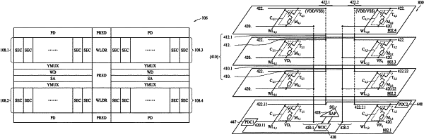
11. A memory device, comprising:
a plurality of circuit layers disposed one above another, each circuit layer comprising one or more memory cells;
a plurality of conductive through via structures penetrating though the circuit layers, the conductive through via structures comprising a first conductive through via structure and a second conductive through via structure separate from the first conductive through via structure;
a data bitline having a plurality of data bitline segments disposed on the circuit layers respectively, the data bitline segments being electrically connected through the first conductive through via structure, the data bitline being coupled to a data memory cell of a first circuit layer; and
a reference bitline having a plurality of reference bitline segments disposed on the circuit layers respectively, the reference bitline segments being electrically connected through the second conductive through via structure, the reference bitline being coupled to a reference memory cell of the first circuit layer, the reference memory cell being accessed when the data memory cell is accessed.
|