| CPC G09G 3/32 (2013.01) [G09G 2300/0809 (2013.01); G09G 2310/061 (2013.01); G09G 2320/0247 (2013.01); G09G 2330/02 (2013.01)] | 20 Claims |
|
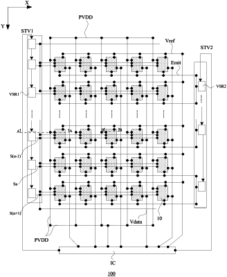
1. A display panel comprising:
a pixel circuit including:
a light emitting module;
a driving module configured to drive the light emitting module, a control end of the driving module being connected to a first node;
a first dual control module, a control end of the first dual control module being connected to a first scanning line, a first end of the first dual control module being connected to the first node, and a first capacitor being formed between an intermediate node of the first dual control module and a first potential line; and
a second dual control module, a control end of the second dual control module being connected to a second scanning line, a first end of the second dual control module being connected to the first node, a second end of the second dual control module being connected to a first end of the driving module, and a second capacitor being formed between an intermediate node of the second dual control module and a second potential line;
wherein at least one of the first capacitor or the second capacitor includes a semiconductor material.
|