| CPC G09G 3/32 (2013.01) [H01L 25/0753 (2013.01); H01L 33/36 (2013.01); H01L 33/62 (2013.01); G09G 2300/0426 (2013.01); G09G 2310/0278 (2013.01); H01L 2933/0016 (2013.01); H01L 2933/0066 (2013.01)] | 15 Claims |
|
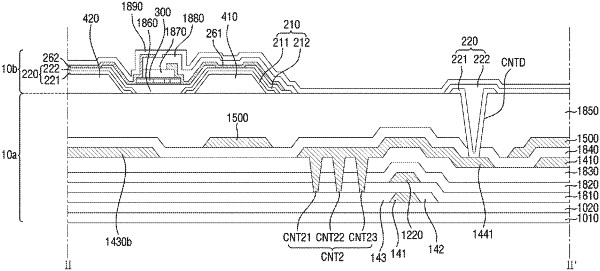
1. A display device comprising:
a substrate;
a circuit element layer on the substrate, the circuit element layer comprising:
a first transistor;
a second transistor comprising a gate electrode connected to a first scan line, and one electrode connected to one electrode of the first transistor;
a third transistor comprising a gate electrode connected to a second scan line, one electrode connected to a gate electrode of the first transistor, and an other electrode connected to a data line; and
a first conductive pattern electrically connected to the one electrode of the first transistor and the one electrode of the second transistor;
a first electrode and a second electrode on the circuit element layer and spaced from each other; and
a light emitting element on the first electrode and the second electrode,
wherein one end of the light emitting element is electrically connected to the first conductive pattern, and
wherein the data line and the first conductive pattern are disposed directly on a same layer.
|