| CPC G09G 3/32 (2013.01) [G09G 3/3266 (2013.01); G09G 2310/0216 (2013.01); G09G 2310/0262 (2013.01)] | 26 Claims |
|
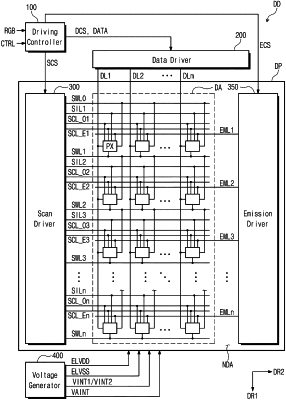
1. A display device comprising:
a display panel including a pixel,
wherein the pixel includes:
a light emitting element;
a first driving transistor connected between a first node and the light emitting element;
a second driving transistor connected between the first node and the light emitting element;
a switching transistor connected between a data line and the first node, and configured to receive a first scan signal;
a first compensation transistor connected between a first control electrode of the first driving transistor and a second node, and configured to receive a first compensation scan signal;
a second compensation transistor connected between a second control electrode of the second driving transistor and the second node, and configured to receive a second compensation scan signal;
a first initialization transistor connected between the first control electrode of the first driving transistor and a first initialization voltage line, and configured to receive a second scan signal; and
a second initialization transistor connected between the second control electrode of the second driving transistor and a second initialization voltage line, and configured to receive the second scan signal.
|