| CPC G06N 3/088 (2013.01) [G06F 18/23 (2023.01); G06N 3/045 (2023.01); G06N 3/047 (2023.01); G06T 7/001 (2013.01); G06V 10/30 (2022.01); G06V 10/431 (2022.01); G06V 10/48 (2022.01); G06V 10/7625 (2022.01); G06V 10/7715 (2022.01); G06T 2207/20081 (2013.01); G06T 2207/20084 (2013.01); G06T 2207/30148 (2013.01)] | 7 Claims |
|
1. A method for detecting a defect pattern on a wafer, the method being performed by a computing device, and comprising:
obtaining binarized inspection data for each wafer including data indicating defectiveness of each of a plurality of chips, the binarized inspection data comprising a first axis coordinate based on a first axis, and a second axis coordinate based on a second axis;
mapping the binarized inspection data to a three-dimensional space based on the first axis, the second axis, and a third axis, wherein third axis coordinates correspond to the data indicating defectiveness;
generating a surface regression model through three-dimensional surface regression constructed by the binarized inspection data mapped to the three-dimensional space;
performing first noise removal based on three-dimensional spatial auto-correlation on the binarized inspection data mapped to the three-dimensional space to generate denoised binarized inspection data, wherein the performing the first noise removal comprises using the surface regression model,
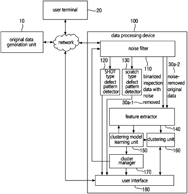
extracting a feature from the denoised binarized inspection data, wherein the feature comprises a feature calculated based on a defective chip distribution pattern obtained as a result of density estimation based on a polar coordinate system of a defective chip; and
performing unsupervised learning for generating a defect pattern clustering model using the feature of the denoised binarized inspection data.
|