| CPC G06K 19/07773 (2013.01) [G06K 19/07771 (2013.01); H01Q 1/2225 (2013.01); H01Q 1/38 (2013.01); H01Q 9/0421 (2013.01); H01Q 13/08 (2013.01)] | 7 Claims |
|
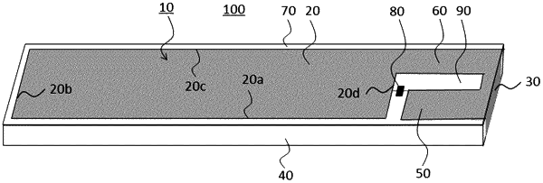
1. An RF tag comprising:
an RF tag antenna; and
an IC chip that operates based on a radio wave,
the RF tag antenna comprising:
an insulation base material having a first main surface, a second main surface facing the first main surface, a first lateral surface adjacent to the first main surface and the second main surface;
a first waveguide element provided on the first main surface;
a second waveguide element provided so as to extend from the second main surface to the first lateral surface and the first main surface;
a power supply part provided on the first main surface, one end of which is electrically connected to the first waveguide element and the other end of which is electrically connected to the second waveguide element and mounted with the IC chip; and
a short circuiting part provided on the first main surface, one end of which is electrically connected to the first waveguide element and the other end of which is electrically connected to the second waveguide element, wherein
the insulation base material, the first waveguide element, the second waveguide element, the power supply part and the short circuiting part constitute a planar inverted-F antenna that receives the radio wave transmitted from a reading device,
the total length of lateral sides of the first waveguide element is 20% or more and 30% or less of a wavelength (λ) of the radio wave, and
an inductance (L) constructed of the first waveguide element, the short circuiting part, the second waveguide element and the power supply part, and a capacitance (C) that is the sum of a capacitance of a capacitor constructed of the first waveguide element, the second waveguide element and the insulation base material and an equivalent capacitance in the IC chip, constitute a resonance circuit that resonates at a frequency (f) of the radio wave, and the lengths of the power supply part and the short circuiting part are set so that the inductance (L) satisfies:
 |