| CPC G06F 3/0412 (2013.01) [G06F 3/047 (2013.01); H10K 50/84 (2023.02); H10K 59/40 (2023.02); H10K 2102/311 (2023.02)] | 17 Claims |
|
1. A touch display panel, comprising:
a substrate, which comprises a display area and a non-display area;
a light-emitting component, which is located within the display area;
an encapsulation layer, which covers the light-emitting component and at least part of the non-display area;
a touch layer, which is located at a side of the encapsulation layer away from the light-emitting component, the touch layer comprising a plurality of touch electrodes; and
a plurality of touch wires, wherein the plurality of touch wires are directly electrically connected to the plurality of touch electrodes, and the plurality of touch wires extend to the non-display area;
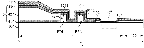
wherein the non-display area comprises a first area and a second area, at least part of film layers within the first area are formed with at least one of a through hole or a groove, the plurality of touch wires extend along a surface of the first area and extend into the second area, and the second area is located at a side of the first area away from the display area;
wherein the non-display area comprises a first organic layer covering the touch wires in the first area; the first organic layer further comprises a plurality of first grooves which are located on a side of the first organic layer away from the touch wires; and
wherein
a first film layer within the first area is formed with the through hole, a second film layer within the first area is formed with the groove, and the plurality of touch wires extend along a first side wall of the through hole, a first side wall of the groove, a bottom surface of the groove, a second side wall of the groove, and a second side wall of the through hole, and extend into the second area.
|