US 11,816,047 B2
Protocol including a command-specified timing reference signal
Ian Shaeffer, Los Gatos, CA (US); and Thomas J. Giovannini, San Jose, CA (US)
Assigned to Rambus Inc., San Jose, CA (US)
Filed by Rambus Inc., San Jose, CA (US)
Filed on Mar. 3, 2021, as Appl. No. 17/191,469.
Application 17/191,469 is a continuation of application No. 16/405,421, filed on May 7, 2019, granted, now 10,970,240.
Application 16/405,421 is a continuation of application No. 15/498,065, filed on Apr. 26, 2017, granted, now 10,331,587, issued on Jun. 25, 2019.
Application 15/498,065 is a continuation of application No. 13/105,798, filed on May 11, 2011, granted, now 9,665,507, issued on May 30, 2017.
Claims priority of provisional application 61/366,806, filed on Jul. 22, 2010.
Prior Publication US 2021/0279191 A1, Sep. 9, 2021
Int. Cl. G06F 13/16 (2006.01); G06F 12/00 (2006.01); G11C 7/10 (2006.01); G11C 7/22 (2006.01)
CPC G06F 13/1689 (2013.01) [G06F 12/00 (2013.01); G11C 7/10 (2013.01); G11C 7/1066 (2013.01); G11C 7/1093 (2013.01); G11C 7/222 (2013.01); G11C 2207/2254 (2013.01)] 21 Claims
OG exemplary drawing
 
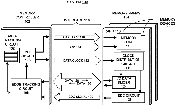
1. A memory controller to a control a memory device, the memory controller comprising:
circuitry to identify an event where the memory device has not transferred data for a least a predetermined idle period;
circuitry to cause, in response to the event, the memory device to commence outputting of a specified timing reference signal prior to transfer of data following passage of the predetermined idle period;
circuitry to calibrate a value of a timing parameter in the memory controller using the specified timing reference signal; and
circuitry to receive the data transferred from the memory device following passage of the predetermined idle period in dependence on the calibrated value of the timing parameter.