| CPC G02F 1/15165 (2019.01) [C09K 9/02 (2013.01); G02F 1/163 (2013.01)] | 19 Claims |
|
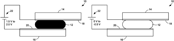
1. An electrochromic device comprising:
an electrically-conducting layer of anodic material;
an electrically-conducting layer of cathodic material;
a single active electrochromic material layer of polymer gel that contains base polymer material, an oxidant configured to cause loss of electrons from the base polymer material, and a colored material that includes a dye,
wherein the single active electrochromic polymer gel material layer is disposed between and in contact with said layer of anodic material and said layer of cathodic material;
wherein the device is configured be alternately placed in a first light-transmitting state, in which relatively large amount of light can be transmitted through the device, and a second light-blocking state, in which relatively small amount of light can be transmitted through the device,
wherein the device comprises no other active layer of material that contributes to transitioning of the device between said first and second light-transmitting states.
|