| CPC G02F 1/13452 (2013.01) [G02F 1/1337 (2013.01); G02F 1/1339 (2013.01); G02F 1/1345 (2013.01); G02F 1/133512 (2013.01); G02F 1/133388 (2021.01)] | 22 Claims |
|
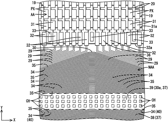
1. A display device comprising:
a display area where images are displayed;
a non-display area that is outside the display area;
substrates each including the display area and the non-display area; and
a liquid crystal layer sandwiched between the substrates;
one of the substrates including:
lines in the display area;
connection lines at intervals in the non-display area;
at least two groups of terminals at intervals in the non-display area;
at least two groups of the connection lines connecting the at least two groups of the terminals and the lines, respectively;
the at least two groups of connection lines including at least two narrow line portions, respectively;
the at least two narrow line portions respectively spreading outwardly with increasing distance from the at least two groups of the terminals;
a wide line portion between the at least two narrow line portions;
pixel electrodes provided in the display area;
an insulation film that covers the wide line portion and the at least two narrow line portions; and
contact holes formed in a portion of the insulation film; and
another one of the substrates including:
a light blocking portion overlapped with the connection lines and the wide line portion in the non-display area, wherein
the wide line portion includes divided lines that are defined by empty portions and are arranged at intervals,
the wide line portion includes a short-circuit portion to short-circuit adjacent divided lines,
a common electrode that is opposite to the pixel electrodes, and
the wide line portion is connected to the common electrode via the contact holes at a portion where the light blocking portion is in the non-display area.
|