| CPC G02F 1/13306 (2013.01) [G02F 1/137 (2013.01); G02F 1/1368 (2013.01); G02F 1/13454 (2013.01); G02F 1/13624 (2013.01); G02F 1/134309 (2013.01); G02F 1/136213 (2013.01); G02F 1/136286 (2013.01); G09G 3/2096 (2013.01); G09G 3/3674 (2013.01); G09G 3/3685 (2013.01); G02F 2202/10 (2013.01); G09G 2300/0426 (2013.01); G09G 2310/0286 (2013.01); G09G 2310/0291 (2013.01); G09G 2330/021 (2013.01)] | 14 Claims |
|
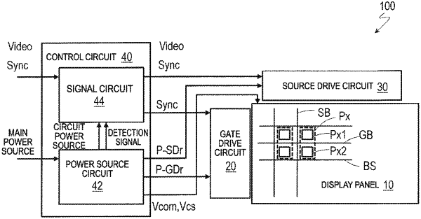
1. A liquid crystal display apparatus comprising:
a plurality of pixels arranged in a matrix having a plurality of pixel rows and a plurality of pixel columns;
a plurality of gate bus lines, each of which is associated with one of the plurality of pixel rows;
a plurality of source bus lines, each of which is associated with one of the plurality of pixel columns; and
a plurality of buffer capacitor scanning lines, each of which is associated with one of the plurality of pixel rows,
wherein each of the plurality of pixels includes
a first liquid crystal capacitor including a first pixel electrode,
a second liquid crystal capacitor including a second pixel electrode,
a first TFT with a drain electrode connected to the first pixel electrode,
a second TFT with a drain electrode connected to the second pixel electrode, and
a buffer capacitor including a buffer capacitor electrode connected to the second pixel electrode via a third TFT,
gate electrodes of the first TFT and the second TFT of each pixel of the plurality of pixels are connected to a gate bus line associated with a pixel row including the pixel,
source electrodes of the first TFT and the second TFT of each pixel of the plurality of pixels are connected to a source bus line associated with a pixel column including the pixel,
a gate electrode of the third TFT of each pixel of the plurality of pixels is connected to a buffer capacitor scanning line associated with a pixel row including the pixel,
the liquid crystal display apparatus further includes
a gate drive circuit configured to supply a gate scanning signal including a first gate-on pulse configured to turn on the first TFT and the second TFT to each of the plurality of gate bus lines, and a buffer capacitor scanning signal including a second gate-on pulse configured to turn on the third TFT to each of the plurality of buffer capacitor scanning lines,
a source drive circuit configured to supply a source signal to each of the plurality of source bus lines, and
a control circuit configured to supply a power source voltage and a control signal to each of the gate drive circuit and the source drive circuit, and
the control circuit is configured to
switch modes from a display mode for normal display to a stop preparation mode in a case that a main power source voltage supplied to the control circuit drops, and
control the gate drive circuit and the source drive circuit to cause
in the display mode, the gate drive circuit to sequentially select the plurality of pixel rows by sequentially applying the first gate-on pulse to the plurality of gate bus lines, and sequentially apply the second gate-on pulse to the plurality of buffer capacitor scanning lines, each of which is associated with the pixel row selected by the first gate-on pulse, during a period that does not overlap a period during which the first gate-on pulse is applied, and the source drive circuit to apply a display signal voltage for normal display to the plurality of source bus lines, and
in the stop preparation mode, the gate drive circuit to sequentially select the plurality of pixel rows by sequentially applying the first gate-on pulse to the plurality of gate bus lines, and sequentially apply the second gate-on pulse to the plurality of buffer capacitor scanning lines, each of which is associated with the pixel row selected by the first gate-on pulse, during a period that at least partially overlaps a period during which the first gate-on pulse is applied, and the source drive circuit to apply 0 V to the plurality of source bus lines.
|