| CPC G02F 1/0305 (2013.01) [H01L 23/055 (2013.01); H05K 1/18 (2013.01); H05K 1/189 (2013.01); G02F 1/055 (2013.01); H05K 2201/10121 (2013.01)] | 7 Claims |
|
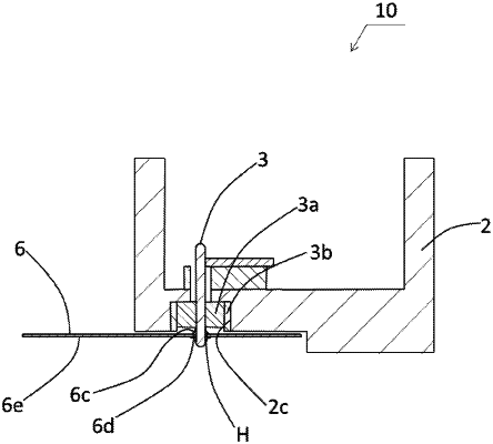
1. A functional element housing package, comprising:
a housing which houses a functional element;
a pin terminal disposed in an outer region of the housing; and
a wiring substrate comprising
a through hole for receiving the pin terminal,
a first metallic layer disposed around an opening of the through hole on a side of the wiring substrate which side is located close to the housing,
a second metallic layer disposed around an opening of the through hole on a side of the wiring substrate which side is opposed to the side located close to the housing, the second metallic layer being greater in area than the first metallic layer,
a connection wiring line connected to the first metallic layer or the second metallic layer, and
a solder which connects the pin terminal to each of the first metallic layer and the second metallic layer.
|