US 11,815,699 B2
Method for producing lens elements and packaged radiation-sensitive devices on wafer level
Norman Laske, Bokelrehm (DE); Hans-Joachim Quenzer, Itzehoe (DE); Vanessa Stenchly, Meldorf (DE); Amit Kulkarni, Hamburg (DE); and Arne Veit Schulz-Walsemann, Oldenborstel (DE)
Assigned to FRAUNHOFER-GESELLSCHAFT ZUR FÖRDERUNG DER ANGEWANDTEN FORSCHUNG E.V., Munich (DE)
Filed by Fraunhofer-Gesellschaft zur Förderung der angewandten Forschung e.V., Munich (DE)
Filed on Oct. 8, 2019, as Appl. No. 16/595,901.
Application 16/595,901 is a continuation of application No. PCT/EP2018/059460, filed on Apr. 12, 2018.
Claims priority of application No. 10 2017 206 387.4 (DE), filed on Apr. 13, 2017; and application No. 10 2017 213 065.2 (DE), filed on Jul. 28, 2017.
Prior Publication US 2020/0041699 A1, Feb. 6, 2020
Int. Cl. B29D 11/00 (2006.01); H01L 31/0232 (2014.01); H01L 31/18 (2006.01); G02B 3/00 (2006.01)
CPC G02B 3/0025 (2013.01) [B29D 11/00298 (2013.01); H01L 31/02327 (2013.01); H01L 31/186 (2013.01)] 31 Claims
OG exemplary drawing
 
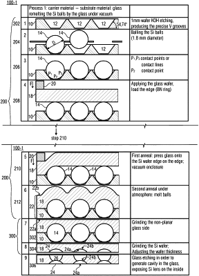
1. A method for producing plano-convex lens elements, comprising:
providing a first partial substrate with ball elements arranged thereon;
providing a second partial substrate comprising a glass material layer;
arranging the second partial substrate on the first partial substrate provided with the ball elements;
fixing the ball elements to the glass material layer of the second partial substrate by means of thermal bonding the ball elements to the glass material layer of the second partial substrate at an increased temperature together with an applied mechanical pressure; and
one-sided thinning of the ball elements fixed to the glass material layer of the second partial substrate to acquire the plano-convex lens elements.