| CPC G01N 27/414 (2013.01) [H01L 29/1087 (2013.01); H01L 29/408 (2013.01); H01L 29/4238 (2013.01); H01L 29/42356 (2013.01)] | 20 Claims |
|
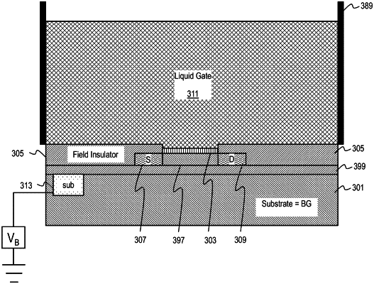
1. An ion-sensitive field effect transistor apparatus, comprising:
a silicon on insulator substrate, in turn comprising a top silicon layer, a buried oxide insulator layer, and a bottom silicon layer a gate insulator spaced outwardly from said substrate, said gate insulator having an exposed outer surface configured for contact with a fluid analyte;
a device region formed in said top silicon layer intermediate said buried oxide insulator layer and said gate insulator;
a source region adjacent said device region;
a drain region adjacent said device region; and
a functionalized layer spaced outwardly of said bottom silicon layer away from said source, said drain, and said device region;
wherein said bottom silicon layer comprises a back gate reference voltage point.
|