| CPC C30B 15/04 (2013.01) [C30B 15/20 (2013.01); C30B 29/06 (2013.01)] | 2 Claims |
|
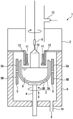
1. A production method of a monocrystalline silicon, comprising:
growing the monocrystalline silicon having a straight-body diameter in a range from 301 mm to 330 mm that is pulled up through a Czochralski process from a silicon melt comprising a dopant in a form of red phosphorus, an inner diameter of a quartz crucible that stores the silicon melt being 1.7 to 2.0 times as large as the straight-body diameter;
pulling up the monocrystalline silicon while rotating the quartz crucible at a rotation speed ranging from 9 rpm to 30 rpm at a start of formation of the straight-body;
changing the rotation speed of the quartz crucible to a range from 0.1 rpm to 7 rpm in a case that the straight-body of the monocrystalline silicon is pulled up from a straight-body start point of the monocrystalline silicon to reach a range from 50 mm to 200 mm;
controlling a resistivity of the monocrystalline silicon at the straight-body start point to fall within a range from 1.20 mΩcm to 1.35 mΩcm; and
subsequently sequentially decreasing the resistivity of the monocrystalline silicon to fall within a range from 0.7 mΩcm to 1.0 mΩcm at a part of the monocrystalline silicon.
|