| CPC B62J 50/21 (2020.02) [G01S 7/526 (2013.01); G01S 15/04 (2013.01); G01S 15/931 (2013.01); H01L 27/0688 (2013.01); H01L 29/7869 (2013.01)] | 12 Claims |
|
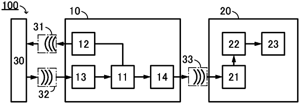
1. A driver alert system comprising:
a first housing comprising:
a first transmission circuit transmitting a first ultrasonic wave;
a first receiving circuit receiving a second ultrasonic wave;
an arithmetic circuit detecting the presence or absence of an object from the second ultrasonic wave; and
a second transmission circuit transmitting a third ultrasonic wave on the basis of a signal obtained in the arithmetic circuit; and
a second housing comprising a second receiving circuit receiving the third ultrasonic wave,
wherein the arithmetic circuit comprises a first selection circuit selecting a potential based on the second ultrasonic wave at a different timing; a plurality of signal retention circuits retaining a potential based on the second ultrasonic wave; a second selection circuit selecting any one of the plurality of signal retention circuits; and a signal processing circuit to which a signal selected in and output from the second selection circuit is input;
wherein each of the plurality of signal retention circuits comprises a first transistor,
wherein the second ultrasonic wave is an ultrasonic wave obtained by reflection of the first ultrasonic wave,
wherein the first transistor comprises a semiconductor layer comprising an oxide semiconductor in a channel formation region,
wherein the second selection circuit selects the plurality of signal retention circuits at different timings to generate a signal obtained by delaying the second ultrasonic wave, and
wherein the third ultrasonic wave generated on the basis of the signal is transmitted to the second housing.
|