| CPC B08B 9/205 (2013.01) [B08B 9/28 (2013.01); F26B 3/30 (2013.01); F26B 21/004 (2013.01); H01L 21/6773 (2013.01)] | 20 Claims |
|
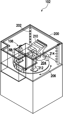
1. A cleaning apparatus for cleaning a wafer carrier that holds wafers as part of a semiconductor fabrication process, the cleaning apparatus comprising:
a wet chamber that receives the wafer carrier to be washed, wherein the wet chamber comprises a clamp configured to couple to a cassette of the wafer carrier when the cassette is separated from a pod of the wafer carrier;
a reservoir in fluid communication with the wet chamber, wherein the reservoir stores a cleaning liquid that is introduced to the wafer carrier within the wet chamber during a washing operation;
a dry chamber spaced apart from the wet chamber, wherein the dry chamber is configured to receive the wafer carrier after the wafer carrier is washed in the wet chamber and hold the wafer carrier during a drying operation; and
a transport system that transports the wafer carrier between the wet chamber and the dry chamber during a cleaning process.
|