| CPC H10N 50/80 (2023.02) [H10B 61/00 (2023.02); H10B 63/00 (2023.02); H10N 50/01 (2023.02); H10N 50/10 (2023.02); H10N 50/85 (2023.02); H10N 70/026 (2023.02); H10N 70/063 (2023.02); H10N 70/231 (2023.02); H10N 70/826 (2023.02)] | 20 Claims |
|
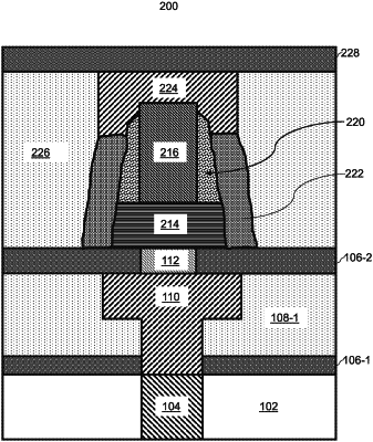
1. A semiconductor device, comprising:
a base structure including a first contact of a memory device;
a memory pillar disposed on the base structure, including:
a conductive central core having a roughness; and
a conductive shell layer surrounding the conductive central core to reduce the roughness;
an encapsulation layer formed on the memory pillar; and
a second contact formed on the memory pillar and the encapsulation layer, wherein the memory pillar includes a cross-section having a parabolic shape.
|