| CPC H10K 59/65 (2023.02) [G01S 17/04 (2020.01); H10K 50/865 (2023.02); H10K 59/121 (2023.02); H10K 59/122 (2023.02); H10K 59/131 (2023.02); H10K 59/38 (2023.02); H10K 59/40 (2023.02); H10K 59/88 (2023.02); G06V 40/19 (2022.01); H04N 23/57 (2023.01)] | 20 Claims |
|
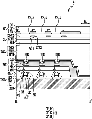
1. A display device comprising:
a display panel including a first region including a transmissive part configured to transmit light provided from the outside and a second region not including the transmissive part; and
a sensor overlapping with the transmissive part, and configured to obtain electrical information based on information provided from the outside,
wherein the display panel includes:
a thin film transistor layer including a plurality of transistors;
a pixel defining layer defining an emission region of a plurality of pixels; and
a light blocking layer on the pixel defining layer, and defining the transmissive part, and
wherein the pixel defining layer in the first region covers at least a portion of the thin film transistor layer such that light provided through the transmissive part is blocked.
|