| CPC H10K 59/131 (2023.02) [G09G 3/3266 (2013.01); G09G 3/3291 (2013.01); H10K 59/122 (2023.02); G09G 2300/0426 (2013.01); H10K 59/1201 (2023.02)] | 21 Claims |
|
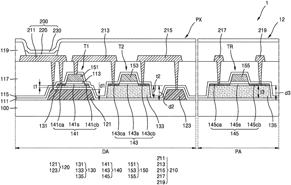
1. A display apparatus comprising:
a substrate;
a conductive mound arranged on the substrate;
a first insulating mound arranged on the substrate; and
a semiconductor layer including a first region arranged on the conductive mound, and a second region arranged on the first insulating mound,
wherein the second region of the semiconductor layer substantially covers an upper surface of the first insulating mound,
wherein the first insulating mound includes organic material.
|
|
12. A display apparatus comprising:
a substrate;
a conductive mound arranged on the substrate;
an organic planarization layer arranged on the substrate and at least partially covering the conductive mound; and
a semiconductor layer arranged on the organic planarization layer and including a first semiconductor region overlapping the conductive mound and a second semiconductor region not overlapping the conductive mound.
|