| CPC H10K 59/131 (2023.02) [H01L 27/1214 (2013.01); H10K 50/00 (2023.02); H10K 59/12 (2023.02); H10K 77/111 (2023.02); H01L 2924/12041 (2013.01); H01L 2924/12044 (2013.01); H10K 50/14 (2023.02); H10K 50/8426 (2023.02); H10K 59/1201 (2023.02); H10K 71/80 (2023.02); H10K 2102/311 (2023.02); Y02E 10/549 (2013.01)] | 12 Claims |
|
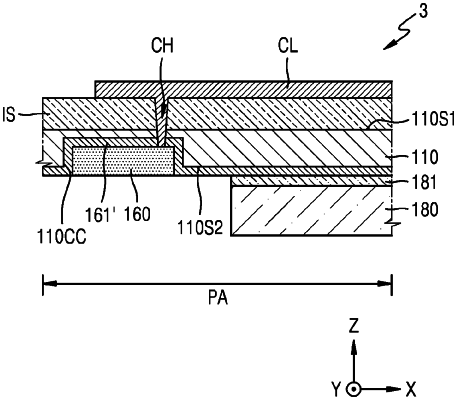
1. A display apparatus comprising:
a conductive pattern comprising a top surface, a bottom surface opposite to the top surface, and a lateral surface connecting the top surface to the bottom surface;
a first adhesion layer covering the top surface and the lateral surface of the conductive pattern;
a first substrate on the first adhesion layer;
a driving circuit over the first substrate, the driving circuit comprising at least one transistor;
a light-emitting device configured to be driven by the driving circuit;
a contact hole formed in the first adhesion layer and the first substrate to partially expose the top surface of the conductive pattern;
a conductive line over the first substrate, the conductive line electrically connecting the driving circuit to the conductive pattern through the contact hole; and
a second substrate under the first adhesion layer, the second substrate exposing the bottom surface of the conductive pattern.
|