| CPC H10K 59/124 (2023.02) [G09G 3/3225 (2013.01)] | 12 Claims |
|
1. An organic-electroluminescent (EL) display apparatus, comprising:
a substrate having a surface with a drive circuit formed on the surface, the drive circuit being formed for each of a plurality of pixels and comprising a thin-film transistor;
a planarizing layer to planarize the surface of the substrate by covering the drive circuit; and
an organic light-emitting element being formed, for each of the plurality of pixels, on a surface of the planarizing layer facing an opposite orientation from the drive circuit, the organic light-emitting element being electrically connected to the drive circuit, wherein
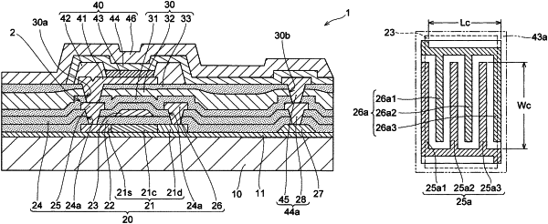
the thin-film transistor comprises a gate electrode, a drain electrode, a source electrode, and a semiconductor layer comprising a region to be a channel of the thin-film transistor and partially overlapping the drain electrode and the source electrode,
a part of a first conductor layer making up the drain electrode and a part of a second conductor layer making up the source electrode are alternately lined up along a given direction,
a plurality of regions each one of which is the region to be the channel is provided and each of the plurality of regions is sandwiched between the part of the first conductor layer and the part of the second conductor layer, and
W/L is 50 or more and 500 or less, wherein the W denotes a sum of lengths of facing portions in the plurality of regions, each of the facing portions being a portion at which the part of the first conductor layer and the part of the second conductor layer face each other, and the L denotes an interval between the first conductor layer and the second conductor layer at the facing portions.
|