| CPC H10K 50/844 (2023.02) [G06F 1/1652 (2013.01); G09F 9/301 (2013.01); H10K 50/8426 (2023.02); H10K 77/111 (2023.02); B32B 2307/54 (2013.01); B32B 2457/206 (2013.01)] | 15 Claims |
|
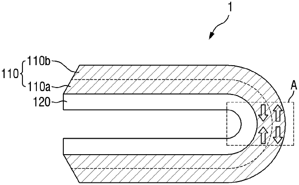
1. A display device comprising:
a substrate;
a light emitting layer on the substrate;
an encapsulation layer on the light emitting layer;
a touch sensing layer on the encapsulation layer;
a cover window on the touch sensing layer; and
a protection film on the cover window,
wherein the protection film includes a base layer and an adhesive layer on the base layer,
the adhesive is disposed between the cover window and the base layer,
the base layer has a modulus of about 2 gigapascals to about 9 gigapascals,
the base layer has a thickness of about 25 micrometers to 75 micrometers,
the adhesive layer has a modulus of about 10 megapascals or less at a temperature of −20 degrees Celsius or lower, and
the adhesive layer has a thickness of 100 micrometers or more.
|