| CPC H10K 50/844 (2023.02) [H10K 59/12 (2023.02); H10K 71/00 (2023.02); H10K 59/1201 (2023.02)] | 14 Claims |
|
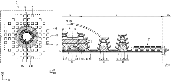
1. A display device comprising:
a substrate including a display area, an opening area positioned in the display area, and a peripheral area positioned between the opening area and the display area;
a transistor positioned in the display area of the substrate;
a first electrode connected to the transistor;
a second electrode positioned on the first electrode;
an inorganic pattern portion positioned in the peripheral area of the substrate; and
an intermediate layer positioned between the first electrode and the second electrode, and including at least one organic layer positioned on the inorganic pattern portion,
wherein:
the inorganic pattern portion includes a plurality of inorganic patterns spaced apart from each other; and
the second electrode does not overlap the inorganic pattern portion.
|