| CPC H10K 50/844 (2023.02) [H10K 59/131 (2023.02); H10K 71/00 (2023.02); H10K 59/1201 (2023.02); H10K 2102/311 (2023.02)] | 17 Claims |
|
1. An electroluminescence display device, comprising:
a substrate divided into a display area and a non-display area;
a power supply line disposed in the non-display area for supplying power supplied to the display area;
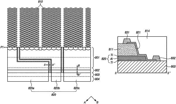
a first insulating film disposed on the power supply line and overlapping a portion of the power supply line and having an open area where a part of the power supply line is exposed;
a conductive film covering the first insulating film and the power supply line in the open area, and
a second insulating film disposed on one end of the conductive film, and on another end of the conductive film located opposite the one end,
wherein the display area comprises:
an active layer;
a gate insulating film disposed on the active layer;
a gate electrode disposed on the gate insulating film and overlapping the active layer;
an interlayer insulating film disposed on the gate insulating film on which the gate electrode is disposed;
a source electrode disposed on the interlayer insulating film and contacting the active layer through a first contact hole formed in the interlayer insulating film;
a drain electrode disposed on the interlayer insulating film and contacting the active layer through a second contact hole formed in the interlayer insulating film;
a protective layer disposed on the interlayer insulating film on which the source electrode and the drain electrode are disposed;
an anode electrode disposed on the protective layer and connected to the source electrode through a third contact hole formed in the protective layer;
a bank formed on the protective layer on which the anode electrode is disposed, and having a cavity overlapping the anode electrode;
a light emitting layer disposed in the cavity;
a cathode electrode disposed on the light emitting layer; and
an encapsulation layer disposed on the cathode electrode, and
wherein the power supply line includes a first power supply line for supplying a first power, a second power supply line for supplying a second power and a reference voltage supply line for supplying a reference voltage, wherein areas in which the first power supply line, the second power supply line and the reference voltage supply line are disposed are divided into a first area, a second area, a third area and a fourth area, respectively, and wherein in the first area and the third area, the protective layer is not placed on the first power supply line, the second power supply line, and the reference voltage supply line; and in the second area and the fourth area, the protective layer is disposed on the first power supply line, the second power supply line, and the reference voltage supply line.
|