| CPC H10K 50/8426 (2023.02) [H10K 59/131 (2023.02); H10K 71/00 (2023.02); H10K 77/10 (2023.02)] | 17 Claims |
|
1. A display device comprising:
a display panel including:
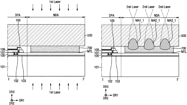
a display area and a non-display area surrounding the display area; and
a metal wiring layer disposed over at least a portion of the non-display area;
an encapsulation substrate disposed on the display panel;
a sealing member which is disposed between the display panel and the encapsulation substrate and bonds the display panel to the encapsulation substrate; and
a first fusion region provided in at least a partial region between the sealing member and the encapsulation substrate,
wherein at least a portion of the sealing member is disposed on the metal wiring layer in the non-display area, and the first fusion region is separated from the metal wiring layer while overlapping the metal wiring layer in a thickness direction,
wherein the first fusion region includes a first portion positioned in parallel with the sealing member and a second portion positioned in parallel with the encapsulation substrate, and
wherein a maximum value of a width of the first portion is greater than a maximum value of a width of the second portion.
|