| CPC H10B 63/84 (2023.02) [H10N 70/826 (2023.02); H10N 70/841 (2023.02)] | 15 Claims |
|
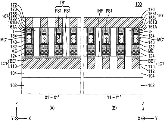
1. A resistive memory device comprising:
a first conductive line extending in a first horizontal direction on a substrate;
a plurality of second conductive lines separated from the first conductive line in a vertical direction and extending in a second horizontal direction, intersecting with the first horizontal direction, on the substrate;
a plurality of memory cells respectively connected between the first conductive line and one second conductive line selected from among the plurality of second conductive lines at a plurality of intersection points between the first conductive line and the plurality of second conductive lines, each of the plurality of memory cells comprising a selection device and a resistive memory pattern; and
a bottom electrode shared by the plurality of memory cells, the bottom electrode having a variable thickness in the first horizontal direction and comprising a top surface having a concave-convex shape;
wherein the bottom electrode is between the first conductive line and the selection device; and
wherein a width of the bottom electrode is less than a width of the selection device in the second horizontal direction.
|